3528 SMD LED Manufacturer for Custom Light Sources
Select a 3528 package around emitter count, red or infrared output, housing design and the space available on your board. Leienda manufactures LED packages and supports their integration into PCB, FPC and PCBA light-source projects.
Explore 3528 Package Options
“3528” identifies a nominal package size class. It does not determine the LED’s voltage, current, power or optical output. Start with the emitter arrangement and package construction, then verify the selected part number against your circuit and optical design.
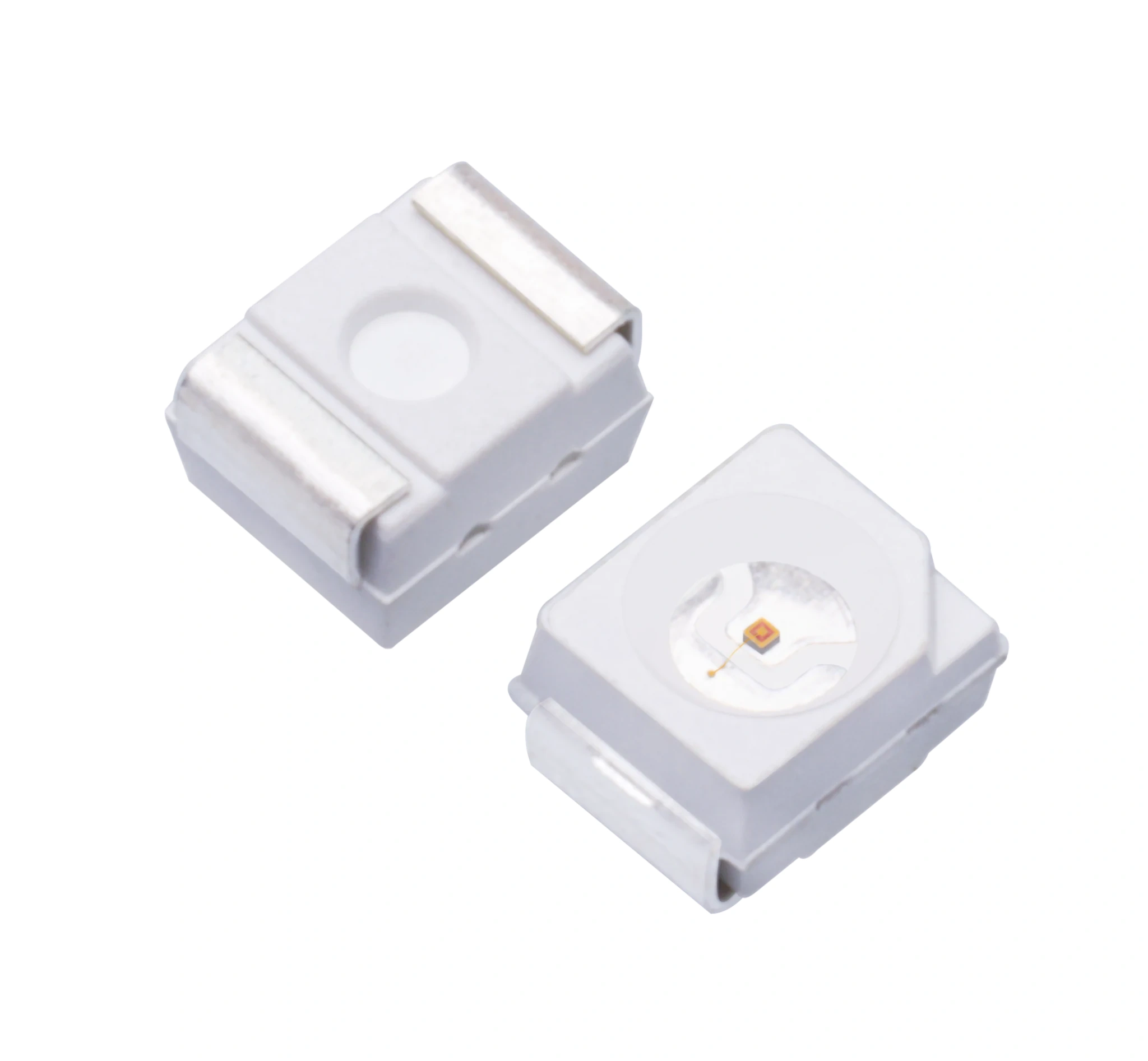
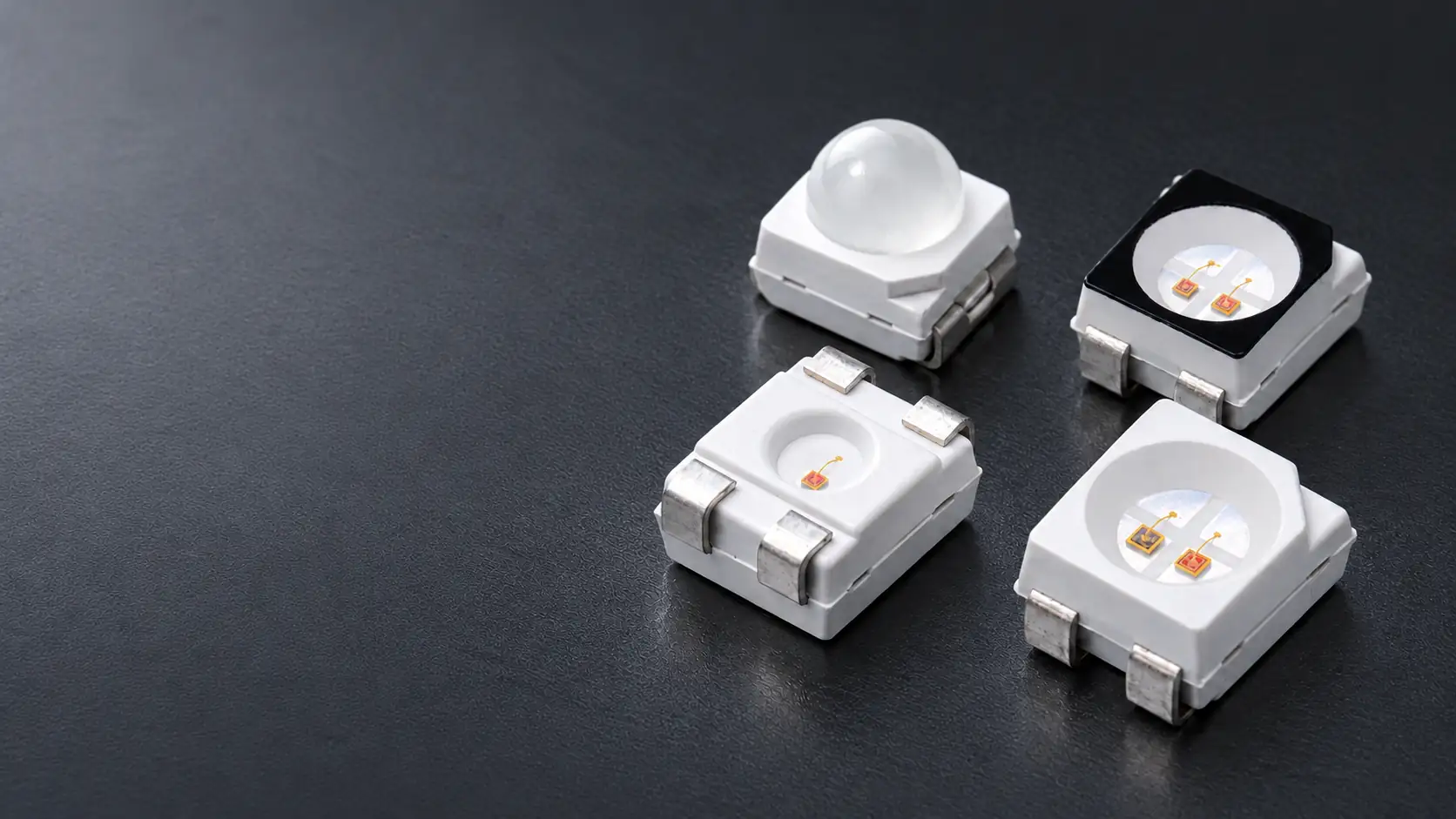
Single-Chip Red 3528 SMD LED
One red emitter in a compact surface-mount package. A starting point for boards that need a single optical channel; confirm the target wavelength, forward voltage and operating current for the selected part.
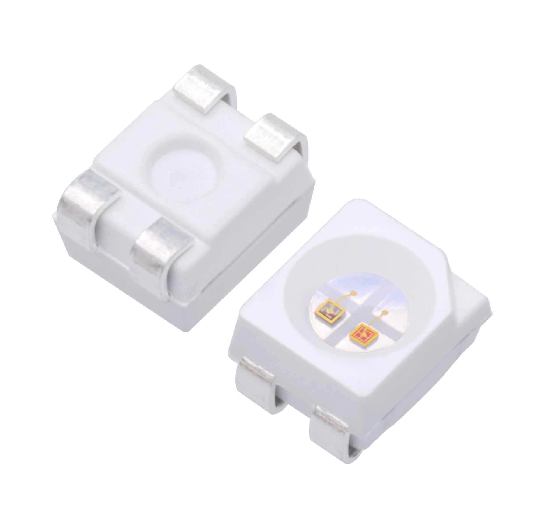
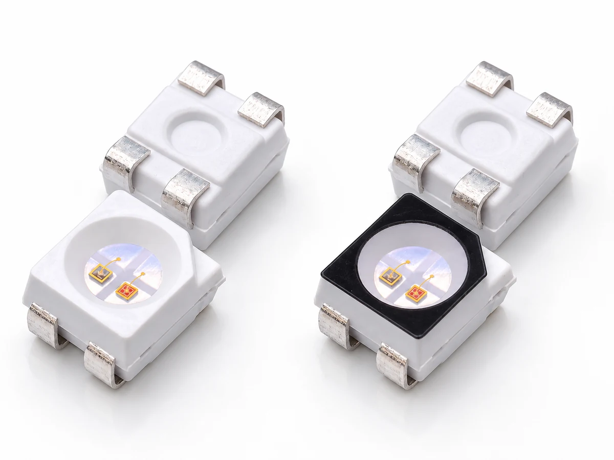
Dual-Chip Red + Infrared 3528 SMD LED
Red and infrared emitters share one package footprint. Evaluate this structure when two optical channels need to fit into a compact board layout; confirm the pinout and drive arrangement before finalizing the PCB.
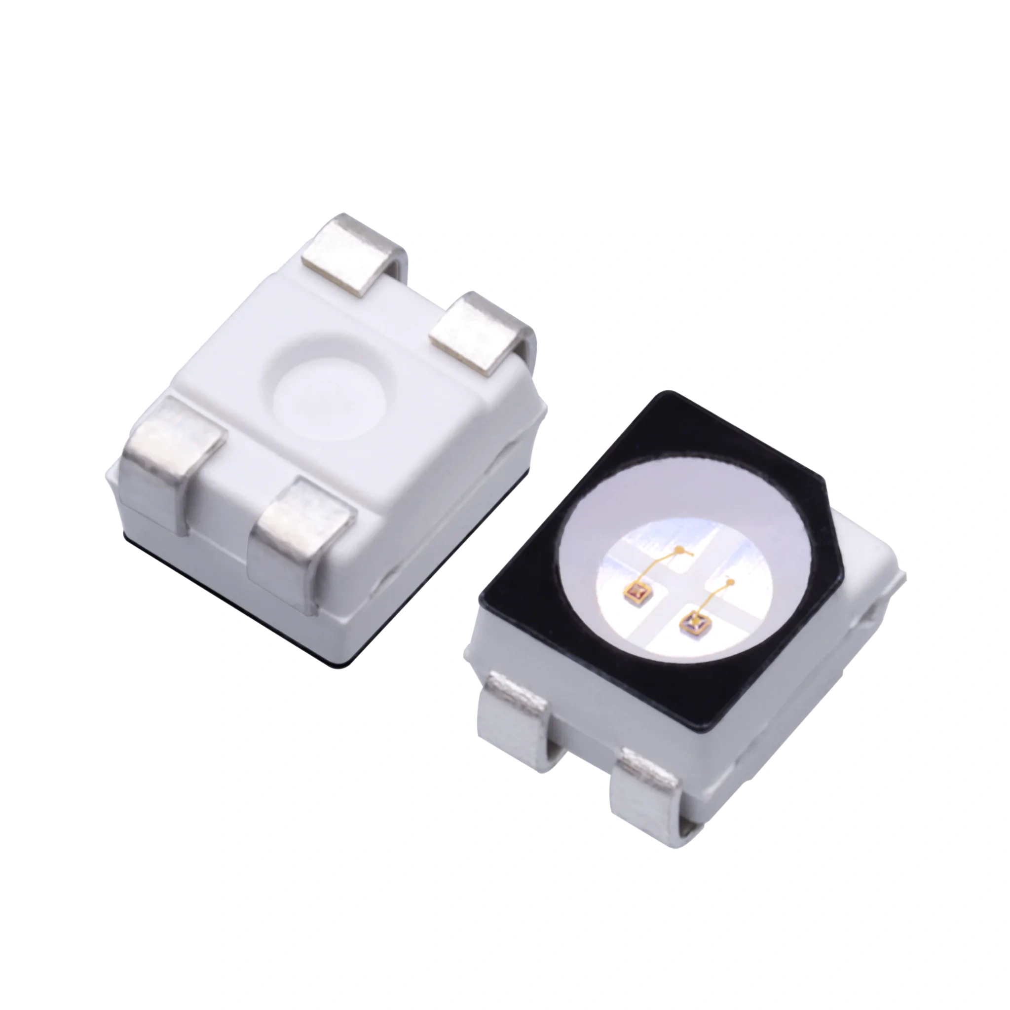
Black-Face Dual-Chip Red + Infrared 3528 SMD LED
A black-face housing option for a red and infrared dual-chip package. Compare its appearance, optical behavior and mechanical fit within the intended enclosure against the standard-face option.
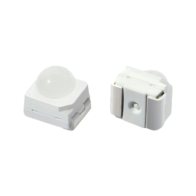
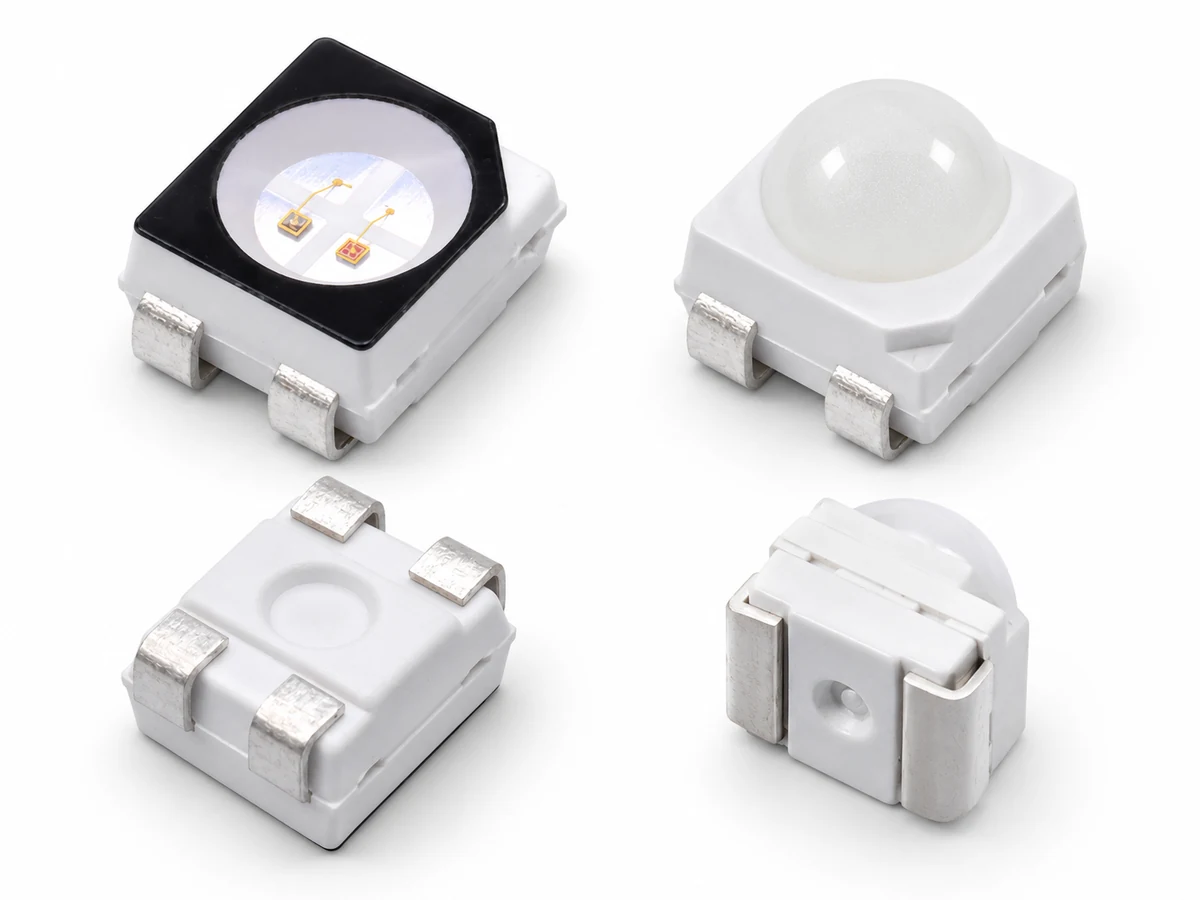
Domed-Top 3528 SMD LED
A molded dome introduces a different package profile. Review beam requirements, lens clearance and board-to-cover distance when considering this construction; available optical and electrical configurations are checked by part number.
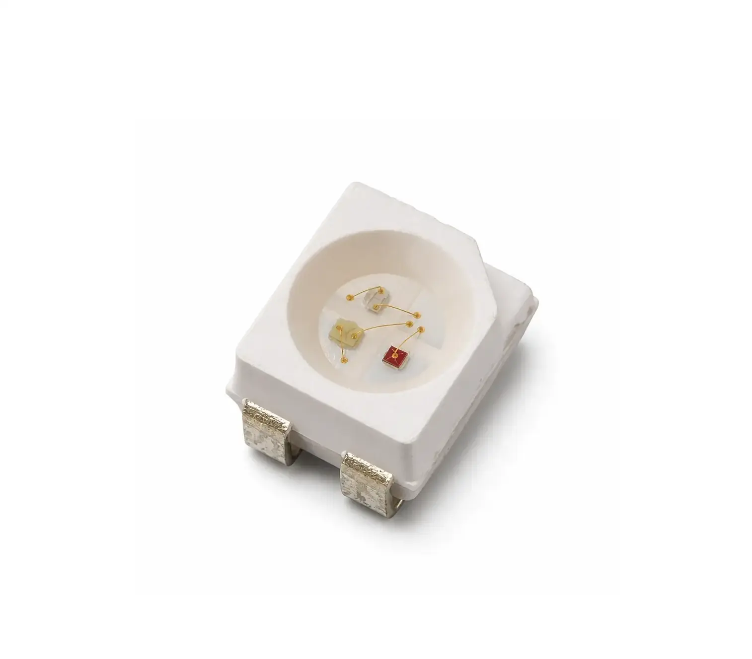
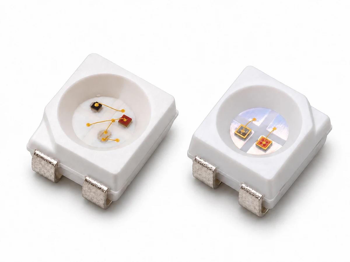
Triple-Chip 3528 SMD LED
A three-emitter construction offers another route for compact multi-channel designs. The emitter combination, pin arrangement, electrical ratings and current supply status require project-specific confirmation.
Design Decisions That Matter Before PCB Release
A package code cannot stand in for a specification
Two 3528 devices may differ in emitter count, wavelength, output and drive conditions. Selecting by the four-digit code alone can leave a board with the wrong optical result or an unsuitable electrical design. Compare candidates at a stated test current and temperature, using the approved part specification.
More emitters change the circuit
A dual-chip, triple-chip or integrated-control device may require a different pad layout, polarity arrangement or control method from a single-chip LED. Check the actual pin diagram and channel-driving requirements before the PCB is released for manufacture.
The lens and board affect the finished light source
A black face and a domed top represent different mechanical and optical choices. Package height, emitter spacing, board material and enclosure clearance should be considered together, especially in compact or shaped light boards.
What to Check in a 3528 SMD LED Specification
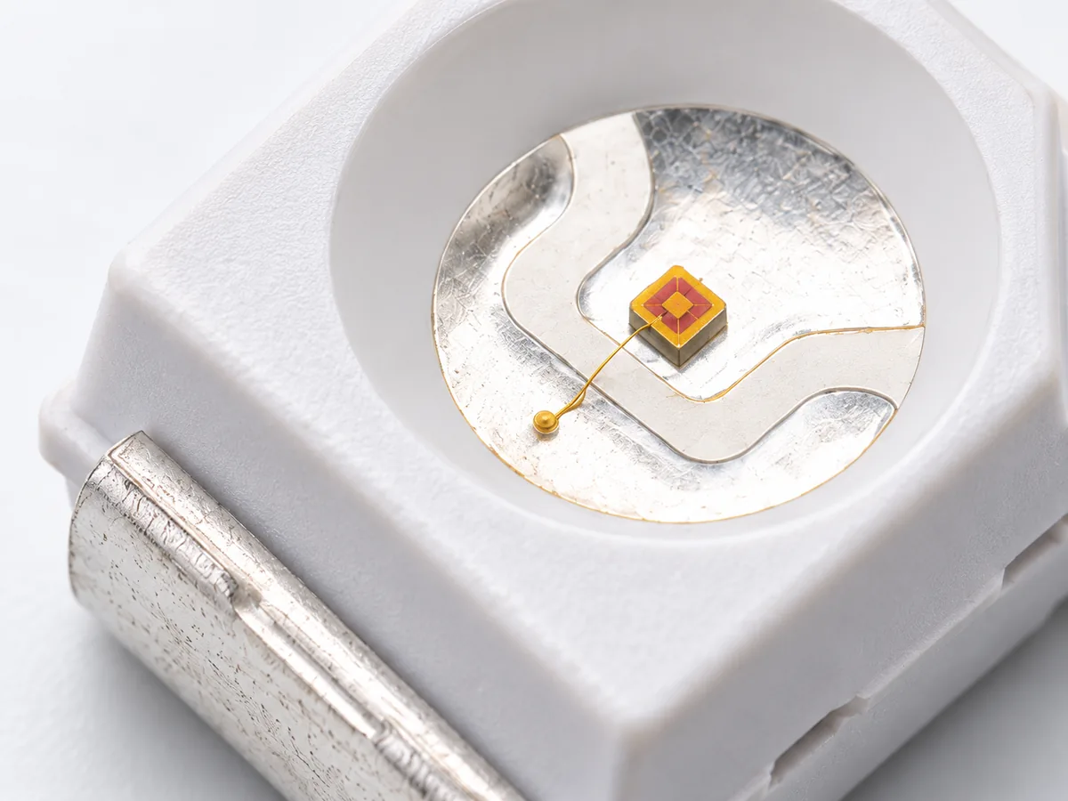
The 3528 code commonly refers to a nominal 3.5 × 2.8 mm package class. Exact outline dimensions, height, pads and tolerances belong to the selected device drawing. There is no universal forward voltage, wattage or lumen value for every 3528 LED.
| Specification field | Why it matters during selection |
|---|---|
| Emitter count and channel arrangement | Determines whether one or several colors or wavelengths share the package, and how they must be driven. |
| Peak or dominant wavelength, or color temperature | Defines the intended optical output; confirm the measurement method and allowable bin for the chosen part. |
| Forward voltage and operating current | Sets the electrical design and the conditions under which output figures should be compared. |
| Optical output and viewing angle | Helps evaluate illumination or radiation at the operating point, together with board spacing and any external optics. |
| Package height, pad layout and polarity | Affects PCB footprint, assembly orientation and clearance inside the enclosure. |
| Thermal and soldering conditions | Connects the LED choice to board design, reflow process and operating environment. |
| Binning, inspection and packaging | Helps define what must remain consistent across approved samples and subsequent production orders. |
Request the part-specific drawing and test conditions before treating a catalog figure as a design limit.
3528 vs 5050: Compare the Complete Device
| Question | 3528 SMD LED | 5050 SMD LED |
|---|---|---|
| Nominal package class | Approximately 3.5 × 2.8 mm | Approximately 5.0 × 5.0 mm |
| Package choice | Useful when board space and the available 3528 emitter arrangement suit the design. | Provides a larger package class for designs that call for a different emitter arrangement or optical target. |
| What the number does not tell you | It does not establish brightness, power, voltage or the number of emitters. | It does not guarantee a brighter or better result in every operating condition. |
| Fair comparison | Compare output at the stated current and temperature, then check beam, board layout and thermal conditions. | Use the same comparison method and evaluate the complete assembled light source. |
Choose the package after defining the required optical output, available PCB area, channel count and operating conditions. If a selected 3528 device cannot meet the system requirement, evaluate an appropriate 5050 option under comparable test conditions.
From 3528 Package Choice to Light-Board Fit

Red and infrared equipment boards
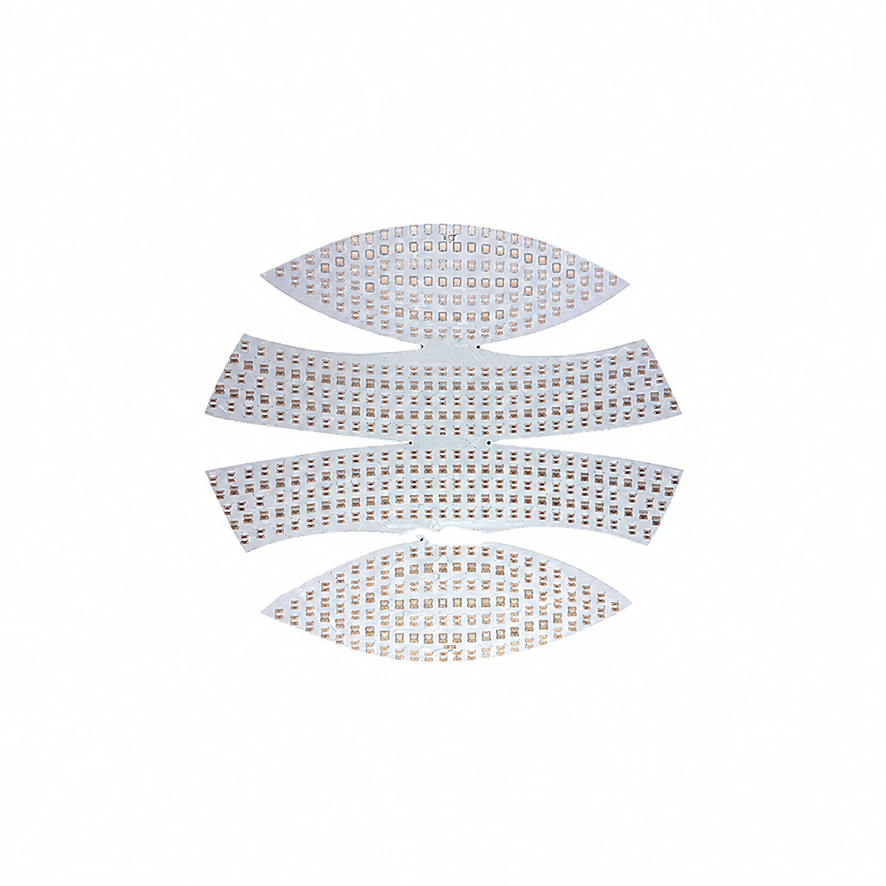
A red and infrared dual-chip package can place two optical channels within one component footprint. For compact equipment boards, review wavelength, channel control, device spacing and the output of the assembled light source together. The finished equipment requires its own optical, thermal and safety validation.
Compact indicators and backlighting
A single-emitter 3528 package may suit equipment indicators or compact backlighting where color, placement and viewing direction matter. Judge the visual result in the actual housing rather than from the package code alone.
Shaped PCB and FPC assemblies
Leienda can discuss the selected LED package alongside a shaped PCB or FPC light board and PCBA assembly scope. Reviewing footprint, polarity, optical layout and assembly needs together helps identify interface issues before board production.
Package and Board Decisions in One Project
More than one 3528 construction
Single-chip, dual-chip, black-face and other documented 3528 structures give the selection process a practical starting point. The final optical and electrical specification is tied to the approved part number.
Coordination beyond the LED package
Package selection can be discussed together with PCB or FPC layout, SMT assembly and PCBA light-source requirements. Reviewing these interfaces early helps reveal footprint, polarity and enclosure conflicts before board production.
A clearer path to sample evaluation
Agree on the parameters that matter to the application—such as wavelength or color, test current, optical output, appearance and packaging—then compare samples against the same stated conditions. Project-specific documents and evaluation scope are confirmed with the selected configuration.
Manufacturing and Inspection in Shenzhen
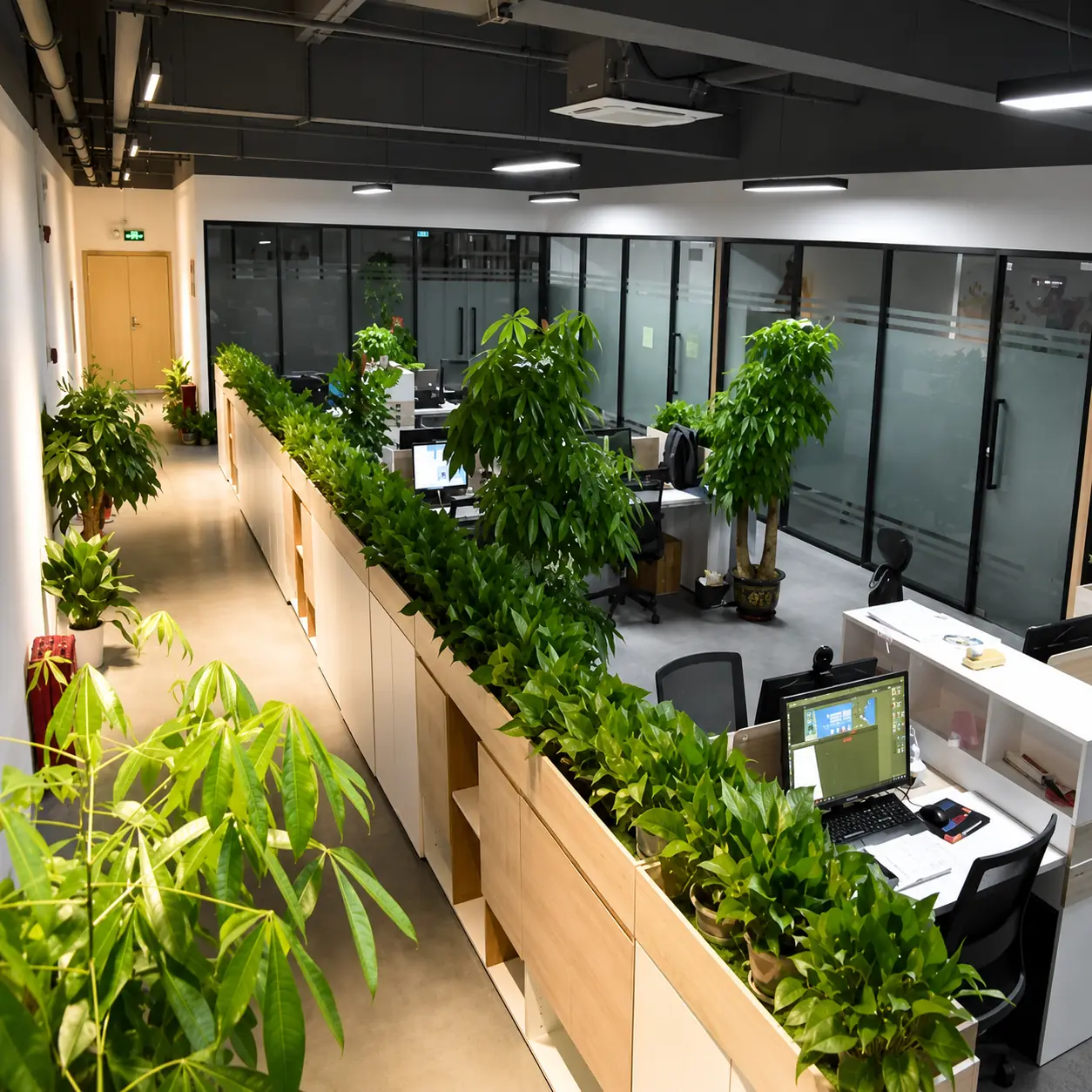
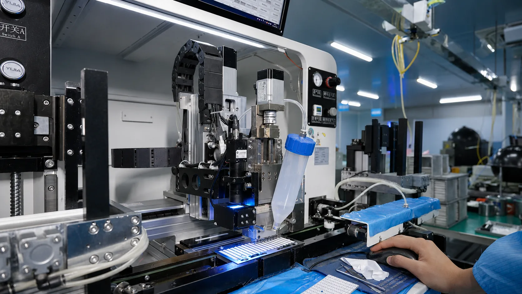
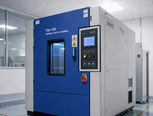
Leienda’s Shenzhen operation covers LED package production and related light-board integration. Incoming-material inspection and finished-product inspection form part of its production workflow.
For a 3528 project, an agreed inspection plan can identify the selected optical and electrical parameters, appearance criteria, package orientation and shipment packaging. Specific test methods, limits and report requirements should be defined for the approved part and order.
3528 SMD LED Selection Guide
What does “3528” tell me?
It identifies a nominal package size class, roughly 3.5 × 2.8 mm. It does not identify a single brightness, voltage, current, wavelength or chip arrangement. The part number and its drawing provide the dimensions and operating limits needed for engineering release.
Is a 3528 LED the same product as a 3528 LED strip?
No. A 3528 SMD LED is a packaged component. A strip is an assembled product whose brightness, voltage and power depend on LED density, circuit design, board construction and other parts. Compare complete strips as systems; compare packaged LEDs by their own specifications and operating conditions.
Can red and infrared emitters share one 3528 package?
Yes, a red and infrared dual-chip structure is among the 3528 options shown here. The package may help when board space is limited, but the exact wavelength, channel arrangement, polarity and drive conditions must be checked against the selected device. A combined package does not remove the need to validate the finished board’s optical and thermal behavior.
How should I choose between a standard face, a black face and a domed top?
Start with the desired optical result and mechanical envelope. Compare how the package looks in the product, how much height is available, and whether a lens or cover changes the beam. Test the candidate in the real enclosure; the face color or dome alone does not establish a guaranteed viewing angle or output.
How should a 3528 LED be driven and mounted?
Use the selected LED’s forward-voltage, current and polarity information to design the circuit. A bare packaged LED should not inherit the voltage rating of a finished strip or module. Before SMT assembly, check the land pattern, orientation, reflow guidance and board thermal path for that exact part.
What should I check when sourcing 3528 LEDs for repeat orders?
Compare suppliers using an identified part number, drawing, optical and electrical test conditions, binning rules, packaging format and agreed inspection criteria. Approve the intended configuration before using its figures in the PCB design or purchasing specification. If the project also needs a shaped PCB, FPC or PCBA light source, define the component-to-board responsibility at the same time.
Discuss Your 3528 LED Configuration
Tell us which package construction you are considering and what the finished light source needs to do. A target wavelength or color, electrical operating point, board drawing and expected quantity will help us review the appropriate component and integration scope. An existing part number is helpful, but it is not required to start the discussion.